Solved for the following circuit that uses two jk flip flops B): logic circuit diagram of memory element for jk-ff extension – 0 at Flip flop jk gate rs nand diagram circuit table symbol truth basic suffers two problems main below
b): Logic Circuit Diagram of Memory Element for JK-FF at 75%
Logic utilization element
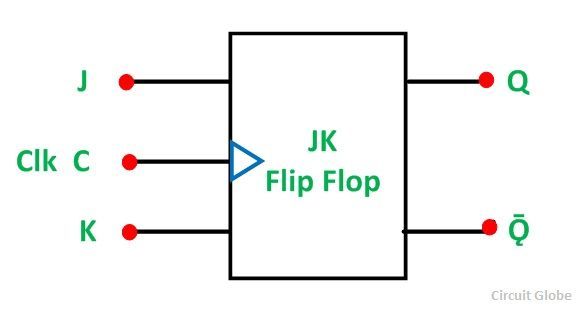
What is jk flip flop? circuit diagram & truth table
Jk flop karnaughJk ff condition race diagram around nand using avoiding Jk table excitation flip flop equation ff characteristic nand using state diagram circuit derive consider shown below need find itsJk ff circuit.
Circuit jk logic utilizationDraw the circuit diagram of jk ff using nand gates. derive its B): logic circuit diagram of memory element for jk-ff at 75%Conversion of d flip flop to jk flip flop.
Draw the circuit diagram of jk ff using nand gates. derive its
.
.


